nesgate
VHDL emulation of the Nintendo Entertainment System
 
Loading...
Searching...
No Matches
logic_core Entity Reference
Inheritance diagram for logic_core:
a_input_register b_input_register mos_6502_alu adder_hold_register

Entities

logic_core.rtl  architecture
 

Ports

adl_bus   inout   std_ulogic_vector ( 7 downto 0 )
  The ADL bus
sb_bus   inout   std_ulogic_vector ( 7 downto 0 )
  The SB bus
db_bus   inout   std_ulogic_vector ( 7 downto 0 )
  The DB bus
control_not_db_add   in   std_ulogic
  NOT(DB)/ADD ALU B Register Load Inverted
control_db_add   in   std_ulogic
  DB/ADD ALU B Register Load
control_adl_add   in   std_ulogic
  ADL/ADD ALU B Register Load ADL Bus
control_sb_add   in   std_ulogic
  SB/ADD - Load from the SB bus into the A input register
control_0_add   in   std_ulogic
  0/ADD - Load 0s into the A input register
control_daa   in   std_ulogic
  DAA - ALU Decimal Mode Enable
control_i_addc   in   std_ulogic
  I/ADDC - ALU Carry-in Input
control_sums   in   std_ulogic
  SUMS - ALU Summation Enable
control_ands   in   std_ulogic
  ANDS - ALU Logical AND Enable
control_ors   in   std_ulogic
  ORS - ALU Logical OR Enable
control_eors   in   std_ulogic
  EORS - ALU Logical XOR Enable
control_srs   in   std_ulogic
  SRS - ALU Shift Right Enable
signal_avr   out   std_ulogic
  AVR - ALU Overflow
signal_carry   out   std_ulogic
  ACR - ALU Carryout
signal_hc   out   std_ulogic
  HC - ALU Half Carry ??
control_add_sb_0_6   in   std_ulogic
  ADD/SB(0-6) - Enable Adder Hold Register SB Bus Outpu, bits 0-6
control_add_sb_7   in   std_ulogic
  ADD/SB(7) - Enable Adder Hold Register SB Bus Outpu, bit 7
control_add_adl   in   std_ulogic
  ADD/ADL - Enable Adder Hold Register ADL Bus Output
metaclock   in   std_ulogic
  Metaclock
phi2   in   std_ulogic
  Ricoh2A03_2A03_Phi2

Detailed Description

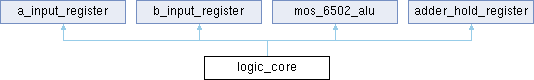
The Arithmetic Logic Unit of the 6502, plus the B and A input registers.

This file combines all the cores of the ALU into one subunit that can be dropped in to a 6502 core. The internal signal routing is handled by this core to minimize the possibility of signal wiring mistakes in higher level designs, and ideally will be optimized out at synthesis time as there's no real logic in this core itself. All actual logic is implemented in the components that this core references.

Member Data Documentation

◆ adl_bus

adl_bus inout std_ulogic_vector ( 7 downto 0 )
Port

◆ control_0_add

◆ control_add_adl

◆ control_add_sb_0_6

◆ control_add_sb_7

◆ control_adl_add

◆ control_ands

◆ control_daa

◆ control_db_add

◆ control_eors

◆ control_i_addc

◆ control_not_db_add

◆ control_ors

◆ control_sb_add

◆ control_srs

◆ control_sums

◆ db_bus

db_bus inout std_ulogic_vector ( 7 downto 0 )
Port

◆ metaclock

metaclock in std_ulogic
Port

◆ phi2

phi2 in std_ulogic
Port

Ricoh2A03_2A03_Phi2

◆ sb_bus

sb_bus inout std_ulogic_vector ( 7 downto 0 )
Port

◆ signal_avr

signal_avr out std_ulogic
Port

◆ signal_carry

signal_carry out std_ulogic
Port

◆ signal_hc

signal_hc out std_ulogic
Port

The documentation for this design unit was generated from the following file: